Laser Thin Film Removal (Patterning)
Thin-film patterning is a selective laser ablation process which allows extremely precise removal of single or multiple layers from a material substrate to create precision circuits.
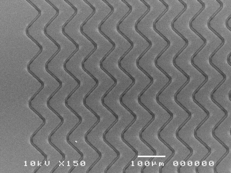
The technique of laser thin-film patterning can produce track and gap widths down to 5µm and with galvo control allowing full design flexibility for one offs to volume production. During the process, the laser beam is scanned over the surface to produce the desired pattern. By altering the number of pulses at each point the depth of mark or pattern can be controlled.
The flexibility of this process is such that it allows for the creation of a wide variety of of features and circuit patterns without the need for a mask. This technique can easily achieve sub-micron selectivity with no damage to the underlying substrate.
An alternative to photolithographic printing, laser thin-film patterning is ideal for rapid prototyping of flexible electronic devices due to the extremely fast process speeds achievable. In addition to contract services, Oxford Lasers also offers a standard system, which can be customised with different laser options, to meet your individual demands.
The use of lasers to pattern a variety of substrates is gaining increasing popularity in a wide variety of sectors. Applications where the removal or patterning of a thin layer, or where the selective removal of multiple layers is key, lend themselves to this form of processing which has advantages over many traditional techniques.
Laser patterning or thin film patterning can not only produce many intricate shapes, but selective ablation allows the removal of layers with thicknesses of less than 100 nanometres.
Particular interest is found in a number of applications from flexible electronics through to applications in the energy and medical sectors.
Dependent on the task at hand, Oxford Lasers have a wide variety of lasers available for laser patterning ranging from ultrafast picosecond and femtosecond lasers through to nanosecond and longer pulsed lasers. Dependent on the application, material and thickness of the layer(s) to be removed, different lasers are used to ensure fast high quality patterning.
Laser Thin Film Removal Specifications | ||
|---|---|---|
Minimum track width |
5µm | |
Materials |
Metals. Most transparent conductive oxide materials (TCOs): from indium tin oxide (ITO) to zinc oxide (ZnO) | |
Research Literature
Mechanistic aspects of selective laser patterning of multilayered thin-film structures in OLED fabrication
Application: OLED, thin-films.
https://www.researchgate.net/publication/265011654_Mechanistic_aspects_of_selective_laser_patterning_of_multilayered_thin-film_structures_in_OLED_fabrication