High Resolution PZT Laser Processing in Medical Ultrasound Device Manufacture
Oxford Lasers has the ability to laser process materials that other micromachining companies struggle to process such as hard ceramics including PZT (piezoelectric ceramics).
PZT is used in the medical device industry in the manufacture of high-resolution ultrasound probes for ultra-precise surgical and medical applications. These high-resolution miniature ultrasound probes are currently manufactured with very complex and expensive processes. Oxford Lasers has introduced a next generation laser micromachining technology for precision structuring of piezoelectric ceramic materials in ultrasound probes. Current technologies either compromise device resolution due to insufficient accuracy (e.g. micro dicing saws), or are very expensive, especially for low volume, customised runs (e.g. lithography).
High precision ultrafast laser micromachining offers a promising alternative which yields high resolution probes at moderate cost. Ultrafast laser micromachining offers minimal heat input during processing which eliminates unwanted depoling. Furthermore, ultrafast laser micromachining can selectively demetallise tracks along user-defined toolpaths without delamination or other deterioration of piezoelectric material performance. Production throughput can be further scaled up by means of laser parallel processing.
Oxford Lasers have been innovating laser micromachining capabilities for over 45 years. Our experience and knowledge have resulted in cutting edge developments to support the advancement in medical device and manufacturing innovation.
If you would like more information, please contact us today.
Precision PZT Laser Processing Advantages
- Simple, quick, low COO, one-step direct write laser process
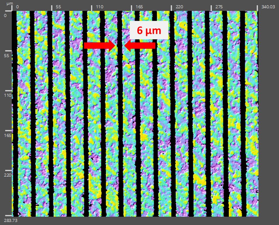
- Precision track cutting/scribing in piezoelectric wafers
- Any track shape possible (straight, curved, zigzag)
- Narrow channels down to <8µm
- No dicing saws
- No lithography, selective laser demetallisation of thin-film electrodes
- No delamination or substrate damage
- No depoling
- No excimer lasers
